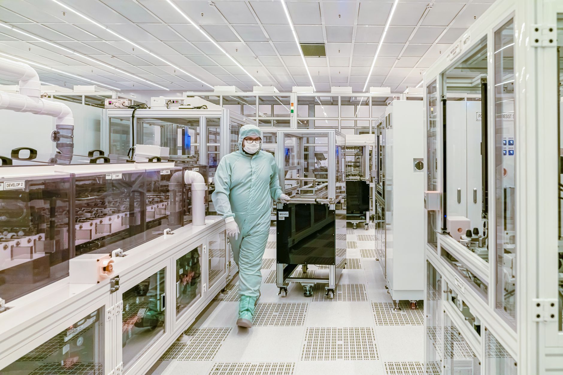
The Dholera semiconductor fab is a chip plant being built by Tata Electronics with Taiwan's PSMC, approved by the Union Cabinet on 29 February 2024 under the India Semiconductor Mission at a reported Rs 91,000 crore (the PIB fiscal support document cites Rs 91,526 crore). It is designed for up to 50,000 wafers a month on 300mm wafers at mature nodes of 28 to 110 nm. Civil work was reported about 50 percent complete by mid-2026, with a first chip targeted for 2026-27. That first-chip date is a target, not an achieved fact.
The Dholera semiconductor fab is a large chip-fabrication plant being built by Tata Electronics in partnership with Taiwan's Powerchip Semiconductor Manufacturing Corporation (PSMC). It was approved by the Union Cabinet on 29 February 2024 under the India Semiconductor Mission (ISM), with a reported investment of Rs 91,000 crore, roughly US$11 billion; the Press Information Bureau (PIB) fiscal support document cites the figure as Rs 91,526 crore. The fab is designed for a capacity of up to 50,000 wafers per month on 300mm wafers, at mature and specialty process nodes ranging from 28 to 110 nm. It is the single anchor that turned Dholera from a planning-map ambition into a nationally significant industrial story.
This page sets out what has actually been approved and built versus what is still a target, because the fab is often described in breathless terms that blur the two. The approvals, investment figure and capacity are durable facts from official sources. The completion status and the first-chip date are moving targets. Keeping that line clear is the whole point. For the wider context, see why Dholera is so famous and the current status of Dholera in 2026.
Who is building the Dholera semiconductor fab?
The fab is being built by Tata Electronics together with PSMC of Taiwan, through an entity named Tata Semiconductor Manufacturing Private Limited (TSMPL). Tata Electronics brings the capital and the on-the-ground execution, while PSMC brings the process technology and foundry know-how, which is the standard shape of a first-time national fab venture: a domestic industrial group paired with an experienced foreign technology partner. The India Semiconductor Mission, the government programme that anchors the country's chip push, backs the project by covering half of the eligible project cost, which is what makes a plant of this scale financially viable at all.
It is worth being precise about names, because the sector is crowded with them. Tata Electronics is the builder here; PSMC is the technology partner; ISM is the central scheme; and TSMPL is the special vehicle that actually holds the project. We stay neutral on the developer itself and simply report what the official record says, without endorsing any company's marketing claims.
How big is the investment and what does the money cover?
The reported investment is Rs 91,000 crore, about US$11 billion, and the PIB fiscal support document specifically cites Rs 91,526 crore. Under the India Semiconductor Mission, the government covers 50 percent of the eligible cost, and the Fiscal Support Agreement that formalises that commitment was signed on 5 March 2025. This is a genuinely large number by Indian industrial standards, and it is one of the reasons the project draws so much attention. It should be understood as the announced project investment, not as a guarantee of returns to anyone buying nearby land, a distinction we come back to below.
Dholera fab: the key numbers
| Item | Detail | Status |
|---|---|---|
| Builder | Tata Electronics with PSMC (entity: TSMPL) | Durable |
| Cabinet approval | 29 February 2024, under ISM | Durable |
| Investment | Rs 91,000 cr (PIB: Rs 91,526 cr) | Durable (reported) |
| Fiscal Support Agreement | Signed 5 March 2025 | Durable |
| Capacity | Up to 50,000 wafers per month, 300mm | Durable design figure |
| Process nodes | 28, 40, 55, 90, 110 nm (mature / specialty) | Durable design figure |
| Civil work | About 50 percent complete | Reported, mid-2026 |
| First chip | 2026-27 | Target, not achieved |
What will the Dholera fab actually make?
The fab is designed for mature and specialty chips rather than the cutting-edge nodes that dominate headlines. It targets process nodes of 28, 40, 55, 90 and 110 nm, and the product families named for it include power-management integrated circuits, display driver chips, microcontroller units and high-performance computing logic. These are the workhorse chips that go into cars, appliances, phones, industrial equipment and countless everyday devices, and global demand for exactly this class of mature-node silicon is deep and durable. In other words, the plant is aimed at a large, real market rather than a narrow, fashionable one.
It is a common misconception that the fab will produce the most advanced processors found in flagship smartphones or data-centre accelerators. It will not; those require sub-10 nm nodes that no Indian fab yet operates. Setting the expectation correctly matters, because the fab's value lies in volume and in building a domestic base in mature nodes, not in leapfrogging to the bleeding edge on day one.
How far along is construction?
As of mid-2026, civil work on the fab was reported to be about 50 percent complete, after a redesign in late 2025 to account for the site's soil conditions. Ground-breaking took place in March 2024, shortly after the Cabinet approval. A significant milestone on the equipment side came with a lithography Memorandum of Understanding (MoU) with ASML, the Dutch lithography-machine maker, reported around 17 May 2026; lithography tools are the heart of any fab, so an ASML relationship is a meaningful signal of intent. Still, an MoU is a statement of intent, not installed machinery, and should be read as such.
The honest summary is that the fab is genuinely under construction, with visible civil progress and a credible equipment partner in the frame, but it is not finished and it is not producing chips. The late-2025 soil redesign is also a reminder that greenfield megaprojects on Dholera's low-lying coastal Bhal land carry real engineering challenges, which is a theme across the region.
When will the first chip be made?
The first chip is targeted for 2026-27, and that word target is doing important work. No official source confirms that a chip has actually been produced at Dholera, and semiconductor fabs are notorious for timeline slippage worldwide, not just in India. A first-chip date is best treated as an aspiration that will be met when it is met, and readers should be sceptical of any claim that presents 2026-27 as a settled fact. When the fab does reach first silicon, it will be a major milestone; until then, it remains a target on a schedule that has already absorbed at least one redesign.
What happened with Vedanta and Foxconn, and where does Micron fit?
Before the Tata project, a different and much-hyped venture collapsed, and it is important not to confuse the two. Vedanta and Foxconn signed an MoU with Gujarat in September 2022 for a semiconductor and display project widely cited at around US$19.5 billion, but Foxconn withdrew from the partnership on 10 July 2023, and that project never built anything. The US$19.5 billion was a headline joint-venture value, not committed capital that was spent, so it should never be presented as money that went into the ground at Dholera.
A separate point of frequent confusion is Micron. Micron's Indian semiconductor assembly and test facility is in Sanand, not Dholera. The two are both in Gujarat and both part of India's chip push, but they are different sites with different companies, and articles that place Micron in Dholera are simply wrong. Getting these distinctions right is part of reading the Dholera story honestly rather than through the fog of marketing.
How many jobs will the fab create?
The Tata fab is officially associated with more than 20,000 direct and indirect jobs, and a broader multi-fab vision has been talked about in terms of around 100,000 jobs as a long-range target. The realistic reading is that the fab will be a significant employer if it reaches full operation, but the larger numbers are aspirations tied to multiple future facilities that do not yet exist. Employment from a single fab also builds up gradually as construction gives way to operations and as an ecosystem of suppliers forms around it, so the jobs arrive over years, not overnight.
Does the fab guarantee that nearby land will appreciate?
No. This is the most important caveat on the page. A large anchor investment can improve an area's prospects, but no government or company source guarantees that land near the fab will rise in value, and anyone promising assured appreciation is selling speculation, not fact. Land prices in Dholera respond to many factors, including scheme status, connectivity and the broader pace of development, and the region's history includes litigation and delays alongside its anchors. Treat the fab as a real and significant project, weigh it against the honest risks in whether Dholera is safe to invest in, and never let a chip factory become the sole basis of a purchase decision.
Why is the India Semiconductor Mission backing this fab?
The India Semiconductor Mission backs the fab because India currently imports almost all of its chips, and a domestic mature-node fab is seen as a first step toward reducing that dependence. The scheme covers 50 percent of the eligible project cost precisely because building a fab is extraordinarily expensive and risky, and no private group would shoulder that alone for a first-of-its-kind national plant. By absorbing half the cost, the government is buying strategic capability: a base of engineers, suppliers and process knowledge that does not exist yet at scale in India. The Dholera fab is the flagship of that policy, which is why its progress is watched as a barometer of the whole mission rather than as one company's project.
This policy framing also explains why the fab landed at Dholera specifically. The region was purpose-built as an industrial node of the Delhi-Mumbai Industrial Corridor, with trunk infrastructure, power and water planned around exactly this kind of heavy, utility-hungry manufacturing. A chip fab needs vast quantities of ultra-pure water, uninterrupted power and clean logistics, and Dholera's plan was designed with those needs in mind, which made it a natural home for the mission's marquee plant.
Why does lithography and the ASML MoU matter?
Lithography is the step that prints circuit patterns onto silicon wafers, and it is the single most critical and expensive class of equipment in any fab, which is why the reported ASML MoU around 17 May 2026 drew so much notice. ASML is the dominant global supplier of lithography systems, and even for mature nodes of 28 to 110 nm, access to reliable lithography tools and support is central to a fab actually working. A relationship with ASML signals that the project is engaging with the tier-one equipment ecosystem rather than improvising, which lends the plan credibility. That said, an MoU is a framework of intent, and the meaningful moment will be tools installed, calibrated and running, not the signing itself. Read the ASML news as encouraging rather than conclusive.
What are the biggest risks and challenges for the fab?
The main challenges are timeline slippage, the technical demands of the site, and the sheer difficulty of running a fab well. Semiconductor plants routinely miss their first-chip dates even in countries with decades of fab experience, so India's first venture of this scale carries obvious execution risk. The late-2025 redesign for soil conditions on Dholera's low-lying coastal land shows that the site itself imposes engineering hurdles, and yield, the share of good chips per wafer, is notoriously hard to ramp on a new line with a new team. There is also the question of the surrounding ecosystem: a fab needs a web of specialised suppliers, chemicals, gases and skilled technicians that India is still building. None of this means the project will fail; it means the honest expectation is a hard, multi-year climb rather than a switch that flips on schedule.
For anyone weighing the fab as a reason to buy nearby, these risks are the counterweight to the excitement. The project is real and substantial, but its most-quoted milestone is still ahead of it, and the region's past includes delays and litigation as well as genuine progress. Balance is the whole discipline here, and it is the reason this page keeps separating the durable approvals from the moving targets rather than blending them into a single confident story.
How does the fab fit into Dholera's bigger picture?
The fab is the flagship anchor of Dholera's industrial thesis, and it sits alongside other real developments such as the operational solar capacity and the new expressway. Dholera was conceived as the largest node of the Delhi-Mumbai Industrial Corridor, and a working chip fab is exactly the kind of high-value manufacturing the whole plan was designed to attract. To see how the pieces connect, read our overview of what Dholera SIR is, the DMIC explained page, and the parallel energy story in the Dholera solar park. Together they show a region where genuine anchors coexist with genuine uncertainty, which is the balanced way to understand the fab: a landmark project, still being built, with its most-quoted milestone still ahead of it.
Frequently asked questions
Who is building the Dholera semiconductor fab?
Tata Electronics is building it with Taiwan's PSMC as technology partner, through an entity called Tata Semiconductor Manufacturing Private Limited. The Union Cabinet approved it on 29 February 2024 under the India Semiconductor Mission, which covers 50 percent of the eligible cost. The Fiscal Support Agreement was signed on 5 March 2025, per PIB.
How much is being invested in the Dholera fab?
The reported investment is Rs 91,000 crore, about US$11 billion, and the PIB fiscal support document cites Rs 91,526 crore. Under the India Semiconductor Mission, the government covers half of the eligible cost. This is an announced project investment and should not be read as any guarantee of returns to nearby land buyers.
What chips will the Dholera fab produce?
It is designed for mature and specialty chips at 28, 40, 55, 90 and 110 nm nodes on 300mm wafers, with capacity up to 50,000 wafers a month. Named product families include power-management ICs, display drivers, microcontrollers and high-performance computing logic. It is not aimed at the cutting-edge sub-10 nm nodes used in flagship smartphone processors.
Has the Dholera fab produced a chip yet?
No. As of mid-2026, civil work was reported about 50 percent complete after a late-2025 soil redesign, and the first chip is targeted for 2026-27. That date is a target, and no official source confirms a chip has been produced. Semiconductor fabs commonly slip on timelines, so treat any firm claim with caution.
Is Micron building a fab in Dholera?
No. Micron's Indian semiconductor facility is in Sanand, not Dholera. Both are in Gujarat and part of India's chip push, but they are different sites with different companies. Articles that place Micron in Dholera are mistaken. The Dholera fab is the Tata Electronics and PSMC project approved in February 2024.
What happened to the Vedanta-Foxconn project?
Vedanta and Foxconn signed an MoU with Gujarat in September 2022, widely cited at about US$19.5 billion, but Foxconn withdrew on 10 July 2023 and the project never built anything. The US$19.5 billion was a headline joint-venture value, not spent capital, so it should not be presented as investment that went into Dholera.
- Press Information Bureau, Government of India (PIB)
- Tata Electronics (tataelectronics.com)
- India Semiconductor Mission (ISM)
- Union Cabinet approval, 29 February 2024
- ASML (asml.com)
The free Dholera First-Timer’s Checklist
Fifteen things to verify before you pay a rupee, in one printable PDF. Written for buyers, not brokers.